2018
論文
- GaAs/GaNAs core-multishell nanowires with nitrogen composition exceeding 2% Mitsuki Yukimune, Ryo Fujiwara, Hiroya Ikeda, Kohsuke Yano, Kyohei Takada, Mattias Jansson, Weimin Chen, Irina Buyanova, and Fumitaro Ishikawa Applied Physics Letters 113, 011901-1-5, 2018.doi:10.1063/1.5029388
- Annealing induced atomic rearrangements on (Ga,In) (N,As) probed by hard X-ray photoelectron spectroscopy and X-ray absorption fine structure Fumitaro Ishikawa, Kotaro Higashi, Satoshi Fuyuno, Masato Morifuji, Masahiko Kondow, Achim Trampert Scientific Reports 8, 5962-1-13, 2018. doi:10.1038/s41598-018-23941-y
- Electronic properties of nano-polycrystalline diamond synthesised by high-pressure and high-temperature technique Rei Fukuta, Fumitaro Ishikawa, Akihiro Ishikawa, Kohsuke Hamada, Masafumi Matsushita, Hiroaki Ohfuji, Toru Shinmei, Tetsuo Irifune Diamond and Related Materials, 84, 66-70, 2018. doi:10.1016/j.diamond.2018.03.007
- エレキテル尾崎財団 源内賞 石川史太郎 「新規半導体ナノワイヤ材料の開拓」,2018年3月25日.
- GaAs/GaNAs core/shell nanowires - a promising platform for nanoscale optoelectronics (I7) S. L. Chen, M. Jansson, F. Ishikawa, W. M. Chen, and I. A. Buyanova Nanowire Week 2018, June 11-15,2018, Hamilton, Canada.
- NPDの電気伝導度制御・ドーピングの試み 石川史太郎 愛媛大学地球深部ダイナミクス研究センター 1st NPD Workshop, 2018年3月1日,愛媛大学.
- Over visible wavelengths polarized light from AlGaOx nanowire (P1.26) Jun Natsui, Naoki Tsuda, Naoki Yamamoto, Fumitaro Ishikawa Nanowire Week 2018, June 11-15,2018, Hamilton, Canada.
- Molecular beam epitaxial growth of GaNAs and GaInNAs nanowires (Tu3.2) M. Yukimune, R. Fujiwara, H. Ikeda, M. Jansson, W. M. Chen, I. A. Buyanova, F. Ishikawa Nanowire Week 2018, June 11-15,2018, Hamilton, Canada.
- Structural investigations on GaAs/GaAsBi core-multishell nanowires (P2.6) Kosuke Yano, Kyohei Takada, Pallavi Patil, Satoshi Shimomura, Yumiko Shimizu, Fumitaro Ishikawa Nanowire Week 2018, June 11-15,2018, Hamilton, Canada.
- Structural Characteristics of GaAs/GaAsBi Nanowires (Fr15PP-NS.2) Kosuke Yano, Kyohei Takada, Pallavi Patil, Satoshi Shimomura, Yumiko Shimizu, Fumitaro Ishikawa Compound Semiconductor Week 2018, May 29–June 1, 2018, Cambridge/Boston, USA.
- Native Oxide AlGaOx Outermost Shell for a Passivation Structure of GaAs‐related Multi‐Layered Nanowires (Fr15PP-NS.5) Naoki Tsuda, Fumitaro Ishikawa Compound Semiconductor Week 2018, May 29–June 1, 2018, Cambridge/Boston, USA.
- Molecular Beam Epitaxial Growth of GaInNAs Nanowires (Fr15PP-NS.6) Mitsuki Yukimune, Hiroya Ikeda, Ryo Fujiwara, Mattias Jansson, Weimin Chen and Irina Buyanova, Fumitaro Ishikawa Compound Semiconductor Week 2018, May 29–June 1, 2018, Cambridge/Boston, USA.
- Growth of GaNAs Nanowires with Nitrogen Concentration over 2Percent (Fr15PP-NS.7) Ryo Fujiwara, Hiroya Ikeda, Mitsuki Yukimune, Mattias Jansson, Weimin Chen and Irina Buyanova, Fumitaro Ishikawa Compound Semiconductor Week 2018, May 29–June 1, 2018, Cambridge/Boston, USA.
- Investigations of Light Polarization of GaAs/AlGaOx Nanowire (Fr15PP-NS.9) Jun Natsui, Naoki Yamamoto, Fumitaro Ishikawa Compound Semiconductor Week 2018, May 29–June 1, 2018, Cambridge/Boston, USA.
- (001)GaAs基板上にMBE成長したGaAsBi/GaAs多重量子井戸の偏光依存PL[17p-F214-11] 樋口 憧生,塚本 晟,伊藤 瑛悟,田中 佐武郎,石川 史太郎,下村 哲 第65回 応用物理学会春季学術講演会, 2017年3月17-20日, 早稲田大学, 東京.
- MBE成長したGaAs/GaAsBi量子井戸のBi組成分布 [17p-F214-12] 塚本 晟,,伊藤 瑛悟,檜垣 興一郎,田中 佐武郎,石川 史太郎,下村 哲 第65回 応用物理学会春季学術講演会, 2017年3月17-20日, 早稲田大学, 東京.
- Si(111) 基板上GaAs/GaAsBiヘテロ構造ナノワイヤにおける微細構造成長 [18p-P8-10] 矢野 康介,高田 恭兵,Patil Pallavi,下村 哲,清水 夕美子,長島 一樹,柳田 剛,石川 史太郎 第65回 応用物理学会春季学術講演会, 2017年3月17-20日, 早稲田大学, 東京.
- AlGaOxナノワイヤの発光特性 [18p-P8-9] 夏井 潤,山本 直紀,石川 史太郎 第65回 応用物理学会春季学術講演会, 2017年3月17-20日, 早稲田大学, 東京.
- 自然酸化AlGaOx最外殻とGaAs/AlGaAsヘテロ構造を用いたGaAsナノワイヤパッシベーション構造の作製 [17p-P1-11] 津田 眞,石川 史太郎 第65回 応用物理学会春季学術講演会, 2017年3月17-20日, 早稲田大学, 東京.
- ダイヤモンド高温・高圧合成時のInP封入効果 [18a-F206-8] 山本 直也,福田 玲,石川 史太郎,松下 正史,新名 享,大藤 弘明,入舩 徹男 第65回 応用物理学会春季学術講演会, 2017年3月17-20日, 早稲田大学, 東京.
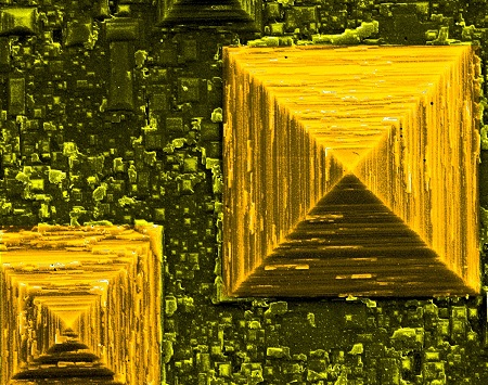
- ダイヤモンド表面に形成された微細ピラミッド構造の観察 [18p-F206-15] 福田 玲,山本 直也,石川 史太郎,松下 正史,大藤 弘明,新名 亨,入舩 徹男 第65回 応用物理学会春季学術講演会, 2017年3月17-20日, 早稲田大学, 東京.
2017
論文
- GaAsBi/GaAs MQWs grown by MBE using a two-substrate-temperature technique Pallavi Kisan Patil, Fumitaro Ishikawa, Satoshi Shimomura Journal of Alloys and Compounds 725, 694, 2017. 10.1016/j.jallcom.2017.07.171
- Morphological and chemical instabilities of nitrogen delta-doped GaAs/(Al, Ga)As quantum wells E. Luna, R. Gargallo-Caballero, F. Ishikawa, and A. Trampert Applied Physics Letters 110, 201906, 2017. 10.1063/1.4983837
- Bismuth flux dependence of GaAsBi/GaAs MQWs grown by molecular beam epitaxy using two-substrate-temperature technique Pallavi Kisan Patil, Fumitaro Ishikawa, Satoshi Shimomura Superlattices and Microstructures, 106, 50, 2017. doi:10.1016/j.spmi.2017.03.021
- Dilute Nitride Nanowire Lasers Based on a GaAs/GaNAs Core/Shell Structure Shula Chen, Mattias Jansson, Jan E. Stehr, Yuqing Huang, Fumitaro Ishikawa, Weimin M. Chen, Irina A. Buyanova Nano Letters, 17, 1775, 2017. doi:10.1021/acs.nanolett.6b05097
- Material conversion of GaAs nanowires Kohei Nishioka, Hidetoshi Suzuki, Kentaro Sakai, Fumitaro Ishikawa Physica Status Solidi b, 254, 1600522, 2017. doi:/10.1002/pssb.201600522
- GaAsBi/GaAs multi-quantum well LED grown by molecular beam epitaxy using a two-substrate-temperature technique Pallavi Kisan Patil, Esperanza Luna, Teruyoshi Matsuda, Kohki Yamada, Keisuke Kamiya, Fumitaro Ishikawa and Satoshi Shimomura Nanotechnology, 28, 105702, 2017. doi:10.1088/1361-6528/aa596c
- Edit
- Novel Compound Semiconductor Nanowires - Materials, Devices, and Applications Fumitaro Ishikawa and Irina A. Buyanova ISBN 978-981-4745-76-5, September 2017, Pan Stanford Publishing Pte. Ltd.
- Chaprters
- GaNAs-Based Nanowires for Near-Infrared Optoelectronics Irina A. Buyanova, Fumitaro Ishikawa, and Weimin M. Chen Chapter 4 in Novel Compound Semiconductor Nanowires - Materials, Devices, and Applications, edited by Fumitaro Ishikawa and Irina A. Buyanova, pp. 133-160, September 2017, Pan Stanford Publishing Pte. Ltd.
- Dilute Bismide Nanowires Wojciech M. Linhart, Szymon J. Zelewski, Fumitaro Ishikawa, Satoshi Shimomura, and Robert Kudrawiec Chapter 5 in Novel Compound Semiconductor Nanowires - Materials, Devices, and Applications, edited by Fumitaro Ishikawa and Irina A. Buyanova, pp. 161-176, September 2017, Pan Stanford Publishing Pte. Ltd.
- GaAs/AlGaOx Heterostructured Nanowires Fumitaro Ishikawa and Naoki Yamamoto Chapter 8 in Novel Compound Semiconductor Nanowires - Materials, Devices, and Applications, edited by Fumitaro Ishikawa and Irina A. Buyanova, pp. 255-290, September 2017, Pan Stanford Publishing Pte. Ltd.
- 応用物理学会秋季学術講演会第10回JSAPフォト&イラストコンテスト 優秀賞
福田玲, 石川史太郎, 山本直也, 松下正史, 大藤弘明, 新名亨, 入舩徹男
「ピラミッドダイヤ」,2017年9月.
- GaAsBi/GaAs量子井戸のMBE成長と発光デバイス試作 下村哲 日本真空学会 2017年9月研究例会,2017年9月26日,愛媛大学.
- Epitaxial nanowires/microstructures exploring next generation electronics Fumitaro Ishikawa STINT/JSPS (The Swedish Foundation for International Cooperation in Research and Higher Education/The Japanese Society for the Promotion of Science) summer workshop 2017,10-12th August, 2017, Viking line cruise between Stockholm-Helsinki, Sweden-Finland.
- Looking for extra compound semiconductor nanowires Fumitaro Ishikawa International Workshop on Advanced Smart Materials and Engineering for Nano- and Bio-Technologies,13-14th July, 2017, Kobe, Japan.
- Pyramid diamond synthesised with high pressure and high temperature technique R. Fukuta, N. Yamamoto, F. Ishikawa, M. Matsushita, H. Ohfuji, T. Shinmei, T. Irifune 28th International Conference on Diamond and Carbon Materials, September 3–7, 2017, Gothenburg, Sweden.
- Analysis of Bi composition of MBE-grown GaAsBi/GaAs quantum wells on GaAs substrates Eigo Ito, Koichiro Higaki, Saburo Tanaka, Pallavi Kisan Patil, Fumitaro Ishikawa, Satoshi Shimomura 8th International Workshop on Bismuth-Containing Semiconductors, July 23–26, 2017, Marburg, Germany.
- Vertically coherent lattice deformation in GaAs/GaAsBi heterostructural nanowires Kyohei Takada, Kosuke Yano, Takeshi Hayakawa, Kohei Nishioka, Pallavi Patil, Fumitaro Ishikawa, Satoshi Shimomura, Kazuki Nagashima, Takeshi Yanagida 8th International Workshop on Bismuth-Containing Semiconductors, July 23–26, 2017, Marburg, Germany.
- Branch formation in GaAs/GaAsBi nanowires on Si(111) Kohsuke Yano, Takeshi Hayakawa, Kyohei Takada, Kohei Nishioka, Pallavi Patil, Fumitaro Ishikawa, Satoshi Shimomura, Kazuki Nagashima, Takeshi Yanagida Compound Semiconductor Week 2017, May 14–18, 2017, Berlin, Germany.
- ダイヤモンド表面処理によるピラミッド型微細構造形成 福田玲, 山本直也, 石川史太郎, 松下正史, 大藤弘明, 新名亨, 入舩 徹男 第58回高圧討論会, 2017年11月8-10日, 名古屋大学, 名古屋.
- GaAs/GaAsBi nanowire growth on Si(111) K. Yano, K. Takada, K. Nishioka, P. Patil, F. Ishikawa, S. Shimomura, K. Nagashima, and T. Yanagida 第36回電子材料シンポジウム (The 36th Electronic Materials Symposium), 2017年11月8-10日, 長浜ロイヤルホテル, 長浜.
- Synthesis of GaAs-related multishell nanowires with native oxide AlGaOx outermost shell N. Tsuda and F. Ishikawa 第36回電子材料シンポジウム (The 36th Electronic Materials Symposium), 2017年11月8-10日, 長浜ロイヤルホテル, 長浜.
- Pyramidal diamond formation by high pressure and high temperature technique R. Fukuta, N. Yamamoto, F. Ishikawa, M. Matsushita, H. Ohfuji, T. Shinmei and T. Irifune 第36回電子材料シンポジウム (The 36th Electronic Materials Symposium), 2017年11月8-10日, 長浜ロイヤルホテル, 長浜.
- レーザー照射によるナノ多結晶ダイヤモンドの表面処理 福田 玲、山本 直也、石川 史太郎、松下 正史、大藤 弘明、新名 亨、入舩 徹男、吉武 剛、池上 浩 第78回応用物理学会秋季学術講演会, 2017年9月5-8日,福岡国際会議場,福岡国際センター,福岡サンパレスホテル, 福岡.
- 高温・高圧処理によるダイヤモンド表面での微細ピラミッド形成 福田 玲、山本 直也、石川 史太郎、松下 正史、大藤 弘明、新名 亨、入舩 徹男 第78回応用物理学会秋季学術講演会, 2017年9月5-8日,福岡国際会議場,福岡国際センター,福岡サンパレスホテル, 福岡.
- 2温度成長法で作製したGaAsBi/GaAs多重量子井戸LEDの温度特性 樋口 憧生、佐々木 大志、塚本 晟、伊藤 瑛悟、山田 光起、パティル パラビ、石川 史太郎、下村 哲 第78回応用物理学会秋季学術講演会, 2017年9月5-8日,福岡国際会議場,福岡国際センター,福岡サンパレスホテル, 福岡.
- GaAs/GaAsBi歪コアーシェルナノワイヤ側壁での垂直格子定数合致型コヒーレント成長 矢野 康介、高田 恭兵、Pallavi Patil、石川 史太郎、下村 哲、長島 一樹、柳田 剛 第78回応用物理学会秋季学術講演会, 2017年9月5-8日,福岡国際会議場,福岡国際センター,福岡サンパレスホテル, 福岡.
- (775)B球面ディンプルGaAs基板上にMBE成長したGaAs/InGaAs 量子井戸の光学的特性 佐々木 大志、橋本 飛鳥、下村 哲 第78回応用物理学会秋季学術講演会, 2017年9月5-8日,福岡国際会議場,福岡国際センター,福岡サンパレスホテル, 福岡.
- GaAs/GaAsBi量子井戸の深さ方向Bi組成の解析 伊藤 瑛悟, 檜垣 興一郎, 田中 佐武郎, Patil Pallavi, 石川 史太郎, 下村 哲 2017 年度応用物理学会中四国支部 若手半導体研究会, 2017年7月29-30日, 愛媛大学, 愛媛.
- GaAs(775)B 基板上における InAs 量子細線の成長モード 佐藤 勇樹, 山田 光起, 下村 哲 2017 年度応用物理学会中四国支部 若手半導体研究会, 2017年7月29-30日, 愛媛大学, 愛媛.
- ダイアモンド高温・高圧合成時の不純物導入の試み 山本直也, 福田玲, 石川史太郎, 松下正史, 大藤弘明, 新名亨, 入舩徹男 2017 年度応用物理学会中四国支部 若手半導体研究会, 2017年7月29-30日, 愛媛大学, 愛媛.
- GaAsBiナノワイヤの成長と評価 矢野康介, 高田恭平, 石川史太郎, 下村哲 2017 年度応用物理学会中四国支部 若手半導体研究会, 2017年7月29-30日, 愛媛大学, 愛媛.
- AlリッチAlGaAsをシェルに持つGaAs/AlGaAsコアーシェル型ナノワイヤの 特性 津田眞, 石川史太郎 2017 年度応用物理学会中四国支部 若手半導体研究会, 2017年7月29-30日, 愛媛大学, 愛媛.
- GaAs/GaAsBiヘテロ構造ナノワイヤの成長機構 高田 恭兵, 西岡 康平, 矢野 康介, 早川 岳志, Patil Pallavi, 石川 史太郎, 下村 哲, 長島 一樹, 柳田 剛 2017 年度応用物理学会中四国支部 若手半導体研究会,2017年7月29-30日, 愛媛大学, 愛媛.
- MBE成長したGaAsBi/GaAs 多重量子井戸LEDの温度特性 樋口憧生, 下村哲, 石川史太郎, Pallavi Patil,伊藤瑛悟, 山田光起, 佐々木大志, 塚本晟, 内山滉貴 2017年度 応用物理・物理系学会 中国四国支部 合同学術講演会, 2017年7月29日, 愛媛大学, 愛媛.
- (100)面GaAs基板上にMBE成長したGaAs/GaAsBi量子井戸のBi組成の解析 塚本晟,伊藤瑛悟,檜垣興一郎,田中佐武郎,Pallavi Patil,石川史太郎,下村哲 2017年度 応用物理・物理系学会 中国四国支部 合同学術講演会, 2017年7月29日, 愛媛大学, 愛媛.
- 球面ディンプルを形成した(775)B GaAs基板上にMBE成長したGaAs/InGaAs 量子井戸の光学特性 佐々木大志, 橋本飛鳥,下村哲 2017年度 応用物理・物理系学会 中国四国支部 合同学術講演会, 2017年7月29日, 愛媛大学, 愛媛.
- 影型マスクアライナーのi線化と画像反転フォトレジストの露光条件 神原 誉,二宮 大吾,若松 将太,上田 耕大,大森隆広,下村 哲 2017年度 応用物理・物理系学会 中国四国支部 合同学術講演会, 2017年7月29日, 愛媛大学, 愛媛.
- 高濃度Al組成AlGaAsをシェルに持つGaAs/AlGaAsコアーシェル型ナノワイヤの 特性 津田眞, 石川史太郎 2017年度 応用物理・物理系学会 中国四国支部 合同学術講演会, 2017年7月29日, 愛媛大学, 愛媛.
- 高温・高圧合成ダイアモンドへの不純物導入 山本直也, 福田玲, 石川史太郎, 松下正史, 大藤弘明, 新名亨, 入舩徹男 2017年度 応用物理・物理系学会 中国四国支部 合同学術講演会, 2017年7月29日, 愛媛大学, 愛媛.
- GaAsBiナノワイヤの成長 矢野康介, 高田恭平, 石川史太郎, 下村哲 2017年度 応用物理・物理系学会 中国四国支部 合同学術講演会, 2017年7月29日, 愛媛大学, 愛媛.
- GaAs(775)B 基板上における InAs 量子細線サイズ分布 山田 光起, 佐藤 勇樹, 下村 哲 第64回 応用物理学会春季学術講演会, 2017年3月14-17日, パシフィコ横浜, 横浜.
- (100)A面 GaAs基板上にMBE成長したGaAs/GaAsBi量子井戸のBi組成の解析 伊藤 瑛悟, 檜垣 興一郎, 田中 佐武郎, Patil Pallavi, 石川 史太郎, 下村 哲 第64回 応用物理学会春季学術講演会, 2017年3月14-17日, パシフィコ横浜, 横浜.
- Si(111) 基板上GaAs/GaAsBiヘテロ構造ナノワイヤの成長機構 高田 恭兵, 西岡 康平, 矢野 康介, 早川 岳志, Patil Pallavi, 石川 史太郎, 下村 哲, 長島 一樹, 柳田 剛 第64回 応用物理学会春季学術講演会, 2017年3月14-17日, パシフィコ横浜, 横浜.
- 高温高圧合成ナノ多結晶ダイヤモンドの光学特性評価 福田 玲, 石川 晃啓, 石川 史太郎, 松下 正史, 大藤 弘明, 新名 亨, 入舩 徹男 第64回 応用物理学会春季学術講演会, 2017年3月14-17日, パシフィコ横浜, 横浜.
- 変質処理によりInを導入させたGaAsナノワイヤの発光特性 中野 真理菜, 合田 拓矢, 碇 哲雄, 西岡 康平, 石川 史太郎, 福山 敦彦 第64回 応用物理学会春季学術講演会, 2017年3月14-17日, パシフィコ横浜, 横浜.
- GaAs/GaAsBiヘテロ構造ナノワイヤの成長時構造変形 石川 史太郎, 高田 恭兵, 西岡 康平, 矢野 康介, 早川 岳志, 下村 哲, 長島 一樹, 柳田 剛 第64回 応用物理学会春季学術講演会, 2017年3月14-17日, パシフィコ横浜, 横浜.
- 高温高圧合成ナノ多結晶ダイヤモンドの電気・光学的特性 石川 史太郎 Workshop on Materials science under ultra-high pressure, 2017年3月2-3日,愛媛大学, 松山.
2016
論文
- (Frontispiece) White-Light Emitters: (Al,Ga)Ox Microwire Ensembles on Si Exhibiting Luminescence over the Entire Visible Wavelength Range Fumitaro Ishikawa, Pierre Corfdir, Uwe Jahn, Oliver Brandt Advanced Optical Materials, 4, 2016, 2016. doi:10.1002/adom.201670068
- (Al,Ga)Ox Microwire Ensembles on Si Exhibiting Luminescence over the Entire Visible Wavelength Range Fumitaro Ishikawa, Pierre Corfdir, Uwe Jahn, Oliver Brandt Advanced Optical Materials, 4, 2017, 2016. doi:10.1002/adom.201600695
- Defect formation in GaAs/GaNxAs1-x core/shell nanowires Jan E. Stehr, Shula Chen, Mattias Jansson, Fumitaro Ishikawa, Weimin M. Chen, Irina A. Buyanova Applied Physics Letters, 109, 203103, 2016. doi:/10.1063/1.4967721
- GaAsBi/GaAs MQWs MBE growth on (411) GaAs substrate Pallavi Kisan Patil, Fumitaro Ishikawa, Satoshi Shimomura Superlattices and Microstructures, 100, 1205, 2016. doi:/10.1016/j.spmi.2016.11.003
- Photoacoustic spectroscopy of absorption edge for GaAsBi/GaAs nanowires grown on Si substrate Szymon J. Zelewski, Jan Kopaczek, Wojciech M. Linhart, Fumitaro Ishikawa, Satoshi Shimomura, Robert Kudrawiec Applied Physics Letters, 109, 182106, 2016. doi:10.1063/1.4966901
- Strongly polarized quantum-dot-like light emitters embedded in GaAs/GaNAs core/shell nanowires S Filippov, M Jansson, J E Stehr, J Palisaitis, P Persson, F Ishikawa, W M Chen, I Buyanova Nanoscale, 8, 15939, 2016. doi:10.1039/C6NR05168E
- GaAsナノワイヤの熱処理による物質変換 西岡康平, 石川史太郎 信学技報 (IEICE Technical Report), 116, CPM2016-28, 19, 2016.
- Structural characterization of AlGaAs:Si/GaAs (631) heterostructures as a function of As pressure Leticia Ithsmel Espinosa-Vega, Miguel Ángel Vidal-Borbolla, Ángel Gabriel Rodríguez-Vázquez, Irving Eduardo Cortes-Mestizo, Esteban Cruz-Hernández, Víctor Hugo Méndez-García, Satoshi Shimomura, David Vázquez-Cortés Journal of Vacuum Science & Technology B, 34, 02L119, 2016. doi:/10.1116/1.4944452
- Core shell carrier and exciton transfer in GaAs/GaNAs coaxial nanowires Shula Chen, Mattias Jansson, Stanislav Filippov, Fumitaro Ishikawa, Weimin M. Chen, Irina A. Buyanova Journal of Vacuum Science & Technology B, 34, 04J104, 2016. doi:10.1116/1.4953184
- Nitride-MBE system for in situ synchrotron X-ray measurements Takuo Sasaki, Fumitaro Ishikawa, Tomohiro Yamaguchi, Masamitu Takahasi Japanese Journal of Applied Physics, 55(5S), 05FB05, 2016. doi:10.7567/JJAP.55.05FB05
- Additional compound semiconductor nanowires for photonics (Invited paper) Fumitaro Ishikawa Proceedings of SPIE, 9755, 975526, 2016. doi:10.1117/12.2208408
- Structural properties of GaNAs nanowires probed by micro-Raman spectroscopy S. Filippov, F. Ishikawa, W. M. Chen, I. A. Buyanova Semiconductor Science and Technology, 31, 025002, 2016. doi:10.1088/0268-1242/31/2/025002
- Perturbation analysis on large bandgap bowing of dilute nitride semiconductors Masato Morifuji, Fumitaro Ishikawa Physica B, 485, 89, 2016. doi:/10.1016/j.physb.2016.01.018
- Anomalous lattice deformation in GaN/SiC(0001) measured by high-speed in situ synchrotron X-ray diffraction Takuo Sasaki, Fumitaro Ishikawa, Masamitu Takahasi Applied Physics Letters, 108, 012102, 2016. doi:/10.1063/1.4939450
- 特願2016-113297: 照明装置 出願人 国立大学法人愛媛大学、 発明者 石川史太郎、矢野稔郎
- GaAsBiナノワイヤの分析 石川史太郎, 赤松良彦,渡辺健太郎,上杉文彦,朝比奈俊輔,Uwe Jahn,下村哲 平成28年度 文部科学省ナノテクノロジープラットフォーム総会, 第2部 H27年度の秀でた利用成果事例紹介,JST東京本部,2016年10月31日.
- Additional GaAs related nanowires Fumitaro Ishikawa JSPS workshop on Japan-Sweden frontiers in spin and photon functionalities of semiconductor nanostructures, August 30-31, 2016, Sapporo, Japan.
- Novel GaNAs and GaNP-Based Nanowires ・Promising Materials for Optoelectronics and Photonics Irina Buyanova, Fumitaro Ishikawa, Charles Tu, Weimin Chen IEEE NANO 2016- 16th International Conference On Nanotechnology, August 22-25, 2016, Sendai, Japan.
- GaAsBi Heterostructured Nanowires Grown by Molecular Beam Epitaxy Fumitaro Ishikawa and Satoshi Shimomura The 7th International Workshop on Bismuth-Containing Semiconductors, July 24-27, 2016, Shanghai, China.
- 化合物半導体エピタキシャル成長を基盤とした新機能ナノワイヤ材料の開拓 石川 史太郎 新化学技術推進協会, 先端化学・材料技術部会 新素材分科会講演会, 東京, 2016年2月29日.
- Additional compound semiconductor nanowires for photonics Fumitaro Ishikawa SPIE Photonics West 2016, February 2016, San Francisco, USA.
- GaAsBi/GaAs MQWs LED Grown by Molecular Beam Epitaxy P. Patil, T. Matsuda, K. Yamada, K. Kamiya, F. Ishikawa, S. Shimomura 32nd North American Molecular Beam Epitaxy, September 18-21, 2016, Saratoga Springs, USA.
- Semi-conductive characteristics of nano-polycrystalline diamond synthesized by high pressure and high temperature technique F. Ishikawa, A. Ishikawa, K. Hamada, M. Matsushita, H. Ohfuji, T. Shinmei, T. Irifune International Conference on Diamond and Carbon Materials, September 4-8, 2016, Montpellier, France.
- GaAsBi/GaAs MQWs LED grown by MBE P. Patil, T. Matsuda, K. Yamada, K. Kamiya, F. Ishikawa, S. Shimomura 19th International Conference on Molecular-Beam Epitaxy, September 4-9, 2016, Montpellier, France.
- Molecular Beam Epitaxy of GaAs/GaAsBi Heterostructure Nanowires Kyohei Takada, Yuto Kubota, Yoshihiko Akamatsu, Pallavi Patil, Fumitaro Ishikawa, Satoshi Shimomura 19th International Conference on Molecular-Beam Epitaxy, September 4-9, 2016, Montpellier, France.
- Characterization of Quantum Dot-Like Emission from GaAs/GaNAs Core/Shell Nanowires Mattias Jansson, Fumitaro Ishikawa, Weimin Chen, Irina Buyanova IEEE NANO 2016- 16th International Conference On Nanotechnology, August 22-25, 2016, Sendai, Japan.
- Electronic characteristics of nano-polycrystalline diamond synthesized by high pressure and high temperature technique: Semi-insulating properties at high temperatures Akihiro Ishikawa, Rei Fukuta, Fumitaro Ishikawa, Masafumi Matsushita, Hiroaki Ohfuji, Toru Shinmei, Tetsuo Irifune The 17th International Conference on High Pressure in Semiconductor Physics (HPSP-17) & Workshop on High-pressure Study on Superconducting (WHS), August 7-10, 2016, Tokyo, Japan.
- GaAsBi/GaAs MQWs LED grown by MBE P. Patil, F. Ishikawa, S. Shimomura The 7th International Workshop on Bismuth-Containing Semiconductors, July 24-27, 2016, Shanghai, China.
- Statistical Investigations on the Development of GaAs/GaAsBi Core-Multi Shell Nanowires Kyohei Takada, Yuto Kubota, Yoshihiko Akamatsu, Pallavi Patil, Fumitaro Ishikawa, Satoshi Shimomura Compound Semiconductor Week, June 26-30, 2016, Toyama International Conference Center, Toyama, Japan.
- Material Conversion of GaAs Nanowires by Post Growth Treatment Kohei Nishioka, Hidetoshi Suzuki, Kentaro Sakai, Fumitaro Ishikawa Compound Semiconductor Week, June 26-30, 2016, Toyama International Conference Center, Toyama, Japan.
- Material Conversion of GaAs Nanowires Kohei Nishioka, Fumitaro Ishikawa 229th ECS Meeting, May 29 - June 2, 2016, San Diego, USA.
- Improved Optical Quality and 1.26μm Light Emission from (411) GaAsBi /GaAs MQWs Grown by MBE P. Patil, F. Ishikawa, S. Shimomura 2016 International Conference on Compound Semiconductor Manufacturing Technology, May 16 - 19, 2016, Miami, USA.
- 可視波長全域で発光する(Al,Ga)Ox マイクロワイヤ群 石川 史太郎, Pierre Corfdir, Uwe Jahn, Oliver Brandt 第77回 応用物理学会秋季学術講演会, 2016年9月13-16日, 朱鷺メッセ, 新潟.
- GaAsナノワイヤの熱処理による物質変換
- 西岡康平,石川史太郎 電子情報通信学会 電子部品・材料研究会 (CPM2016), 2016年7月22-23日, 愛媛大学, 松山.
- Semi-conducting characteristics of nano-polycrystalline diamond synthesized by high pressure and high temperature technique Akihiro Ishikawa, Rei Fukuta, Fumitaro Ishikawa, Masafumi Matsushita, Hiroaki Ohfuji, Toru Shinmei, Tetsuo Irifune 第35回電子材料シンポジウム (The 35th Electronic Materials Symposium), 2016年7月6-8日, ラフォーレ琵琶湖, 守山.
- Growth of GaAs/GaAsBi Heterostructure Nanowires by Molecular Beam Epitaxy K. Takada, Y. Kubota, Y. Akamatsu, P. Patil, F. Ishikawa, S. Shimomura 第35回電子材料シンポジウム (The 35th Electronic Materials Symposium), 2016年7月6-8日, ラフォーレ琵琶湖, 守山.
- Post Growth Material Conversion of GaAs Nanowires Kohei Nishioka, Fumitaro Ishikawa 第35回電子材料シンポジウム (The 35th Electronic Materials Symposium), 2016年7月6-8日, ラフォーレ琵琶湖, 守山.
- ディンプル研磨した(411)A GaAs基板上のGaAs/InGaAs量子井戸のMBE成長 橋本 飛鳥、下村 哲 第63回応用物理学会春季学術講演会, 2016年3月19-22日, 東工大大岡山キャンパス, 東京.
- GaAs(775)B基板上におけるInAsの成長モード 佐藤 勇樹、下村 哲 第63回応用物理学会春季学術講演会, 2016年3月19-22日, 東工大大岡山キャンパス, 東京.
- MBE growth for high quality GaAsBi/GaAs MQWs for longer wavelength emission Patil Pallavi、Ishikawa Fumitaro、Shimomura Satoshi 第63回応用物理学会春季学術講演会, 2016年3月19-22日, 東工大大岡山キャンパス, 東京.
- GaAsナノワイヤの成長後物質変換 西岡康平、石川史太郎 第63回応用物理学会春季学術講演会, 2016年3月19-22日, 東工大大岡山キャンパス, 東京.
- 高温高圧合成ナノ多結晶ダイヤモンドの基礎物性評価 石川晃啓、濱田幸佑、石川 史太郎、松下正史、大藤弘明、新名亨、入舩徹男 第63回応用物理学会春季学術講演会, 2016年3月19-22日, 東工大大岡山キャンパス, 東京.
- 分子線エピタキシーによるSi(111) 基板上GaAs/GaAsBiコア-シェルナノワイヤ成長 石川史太郎、赤松良彦、渡辺健太郎、上杉文彦、朝比奈俊輔、Jahn Uwe、下村 哲 第63回応用物理学会春季学術講演会, 2016年3月19-22日, 東工大大岡山キャンパス, 東京.
- Si(111)基板上GaAs/GaAsBi マルチコアーシェルナノワイヤの特性 石川史太郎、赤松良彦、渡辺健太郎、上杉文彦、朝比奈俊輔、Jahn Uwe、下村 哲 第63回応用物理学会春季学術講演会, 2016年3月19-22日, 東工大大岡山キャンパス, 東京.
- その場放射光X線回折によるMBE成長窒化物半導体のひずみ緩和観測 佐々木 拓生、出来 亮太、石川 史太郎、山口 智広、高橋 正光 第63回応用物理学会春季学術講演会, 2016年3月19-22日, 東工大大岡山キャンパス, 東京.
2015
論文
- Growth of GaAsBi/GaAs Multi Quantum Wells on (100) GaAs Substrates by Molecular Beam Epitaxy P. Patil, T. Tatebe, Y. Nabara, K. Higaki, N. Nishii, S. Tanaka, F. Ishikawa, S. Shimomura e-Journal of Surface Science and Nanotechnology, 13, 469, 2015.10.1380/ejssnt.2015.469
- Metamorphic GaAs/GaAsBi heterostructured nanowires F. Ishikawa, Y. Akamatsu, K. Watanabe, F. Uesugi, S. Asahina, U. Jahn, and S. Shimomura Nano Letters, 15, 7265, 2015.doi:10.1021/acs.nanolett.5b02316
- Suppression of non-radiative surface recombination by N incorporation in GaAs/GaNAs core/shell nanowires S. L. Chen, W. M. Chen, F. Ishikawa, and I. A. Buyanova Scientific Reports, 5, 11653, 2015. doi:10.1038/srep11653
- Si-doped AlGaAs/GaAs(6 3 1)A heterostructures grown by MBE as a function of the As-pressure Víctor-Hugo Méndez-Garcíaa, S. Shimomurab, A.Yu. Gorbatchev, E. Cruz-Hernández, D. Vázquez-Cortés Journal of Crystal Growth, 425, 85, 2015. doi:10.1016/j.jcrysgro.2015.03.022 招待講演・特別講演
- Exploring additional functions of GaAs-related nanowires Fumitaro Ishikawa PACIFICHEM 2015, Honolulu, USA, December 2015.
- Semiconductor/oxide composite nanowires supplying white luminescence F. Ishikawa, N. Yamamoto The 228th ECS Meeting, Phoenix, USA, October 2015.
- Molecular Beam Epitaxial Growth of GaAsBi Nanowires on Si(111) Yoshihiko Akamatsu, Fumitaro Ishikawa and Satoshi Shimomura Compound Semiconductor Week 2015, June 28 - July 2, 2015, Santa Barbara, USA
- Characterization of GaAs/GaNAs core/shell nanowires by means of Raman scattering spectroscopy S. Filippov, F. Ishikawa, W. M. Chen, I. A. Buyanova E-MRS 2015 Spring Meeting, May 11-15, 2015, Lille Grand Palais, France.
- Arsenic pressure Dependence GaAsBi/GaAs Growth on (411)B and (100) GaAs Substrates by Molecular Beam Epitaxy Pallavi Patil, Satoshi Shimomura 第76回 応用物理学会秋季学術講演会, 2015年9月13-16日, 名古屋国際会議場, 名古屋.
- 球状ディンプル研磨した(775)B GaAs基板上のGaAs/InGaAs量子井戸のMBE成長 橋本 飛鳥、下村 哲 第76回 応用物理学会秋季学術講演会, 2015年9月13-16日, 名古屋国際会議場, 名古屋.
- GaAs (775) B面基板上のInAsのMBE成長 佐藤 勇樹、下村 哲 第76回 応用物理学会秋季学術講演会, 2015年9月13-16日, 名古屋国際会議場, 名古屋.
- ディンプル研磨したGaAs基板上のMBE成長 橋本 飛鳥、下村 哲 2015年度 応用物理・物理系学会 中国四国支部 合同学術講演会, 2015年8月1日, 徳島大学常三島キャンパス, 徳島.
- (7 7 5)B GaAs基板面上におけるInAsのMBE成長における成長モード 佐藤 勇樹、下村 哲 2015年度 応用物理・物理系学会 中国四国支部 合同学術講演会, 2015年8月1日, 徳島大学常三島キャンパス, 徳島.
- Investigations on the properties of nano-polycrystalline diamond synthesized by high pressure and high temperature technique Kohsuke Hamada, Akihiro Ishikawa, Masashi Matsushita, Fumitaro Ishikawa, Hiroaki Ohfuji, Toru Shinmei, and Tetsuo Irifune 第34回電子材料シンポジウム (The 34th Electronic Materials Symposium), 2015年7月15-17日, ラフォーレ琵琶湖, 守山.
- Semiconductor/oxide composite nanowires providing white luminescence Fumitaro Ishikawa, Naoki Yamamoto 第34回電子材料シンポジウム (The 34th Electronic Materials Symposium), 2015年7月15-17日, ラフォーレ琵琶湖, 守山.
- (100)A面 GaAs基板上のGaAs/GaAsBi超格子のBi組成プロファイルの解析 檜垣 興一郎、西井 寅貴、パラビ パティル、石川 史太郎、下村 哲 第62回 応用物理学会春季学術講演会, 2015年3月11-14日, 東海大学 湘南キャンパス, 神奈川.
- (100)面 GaAs基板上のGaAs/GaAsBi量子井戸のMBE成長 西井 寅貴、檜垣 興一郎、Patil Pallavi、石川 史太郎、下村 哲 第62回 応用物理学会春季学術講演会, 2015年3月11-14日, 東海大学 湘南キャンパス, 神奈川.
- (775)B InP 基板上にMBE成長したInGaAs層のコラゲーションと光学的特性のIn組成依存性 松田 晃賢、下村 哲、森貞 俊 第62回 応用物理学会春季学術講演会, 2015年3月11-14日, 東海大学 湘南キャンパス, 神奈川.
- Si(111)基板上GaAsBiナノワイヤの分子線エピタキシャル成長 赤松 良彦、石川 史太郎、下村 哲 第62回 応用物理学会春季学術講演会, 2015年3月11-14日, 東海大学 湘南キャンパス, 神奈川.
2014
論文
- Selective synthesis of compound semiconductor/oxide composite nanowires H. Hibi, M. Yamaguchi, N. Yamamoto, and F. Ishikawa Nano Letters, 14, 7024, 2014.doi:/abs/10.1021/nl503385g
- Origin of radiative recombination and manifestations of localization effects in GaAs/GaNAs core/shell nanowires S. L. Chen, S. Filippov, F. Ishikawa, W. M. Chen, I. A. Buyanova Applied Physics Letters, 105, 253106, 2014.
- Dielectric-rod photonic crystals improving luminescence from tensile-strained compound semiconductor quantum wells F. Ishikawa, H. Goto, M. Morifuji Applied Physics Express, 7, 112003, 2014.
- Studying the formation of nitrogen δ-doped layers on GaAs(001) using reflection high-energy electron diffraction S. Nishimoto, M. Kondow, F. Ishikawa Journal of Vacuum Science & Technology B, 32, 02C121, 2014.
- Effects of growth interruption, As and Ga fluxes, and nitrogen plasma irradiation on the molecular beam epitaxial growth of GaAs/GaAsN core-shell nanowires on Si(111) N. Ahn, Y. Araki, M. Kondow, M. Yamaguchi, and F. Ishikawa Japanese Journal of Applied Physics, 53, 065001, 2014.
- ナノスケール結晶成長による新機能半導体材料の創出 石川史太郎 月刊 愛媛ジャーナル,137, 80, 2014. 招待講演・特別講演
- 化合物半導体ナノワイヤを基盤とした新光電変換材料探索 石川史太郎 平成26年度 第39回 太陽光発電プロジェクト講演会, 宮崎大学, 宮崎, 2015年 3月.
- Compound semiconductor/oxide composite nanowire system Fumitaro Ishikawa BIT's 4th Annual World Congress of Nano Science and Technology, Qingdao, China, October 2014.
- 窒化物MBEにおける基礎検討事項:~GaAs系結晶成長との比較から~ 石川史太郎 平成26年度 文部科学省ナノテクノロジープラットフォーム 微細構造解析プラットフォーム 第1回放射光利用研究セミナー, 大阪, 2014年9月.